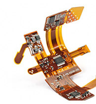
High frequency microwave PCB circuit board exposure has two types: line exposure and solder mask exposure. The function is to cure the irradiated local area through ultraviolet light irradiation, and then develop it to form a circuit pattern or a solder resist pattern.
The process of circuit exposure is to put a photosensitive film on the copper clad board, and then put it together with the circuit pattern negative and expose it with ultraviolet rays. The photosensitive film irradiated by ultraviolet rays will undergo polymerization reaction. The photosensitive film here can resist Na2CO3 weak alkali during development. The solution is washed away, and the non-sensitized part will be washed away during development. In this way, the circuit pattern on the negative film is successfully transferred to the copper clad board;

The process of solder mask exposure is the same: apply photosensitive paint on the circuit board, and then cover the area that needs to be soldered during exposure, so that the pads are exposed after development.

 EN
EN


 Whatsapp 0086 755 29438407
 Mail info@ALPCB.com
  Tel 0086 755 29438407


